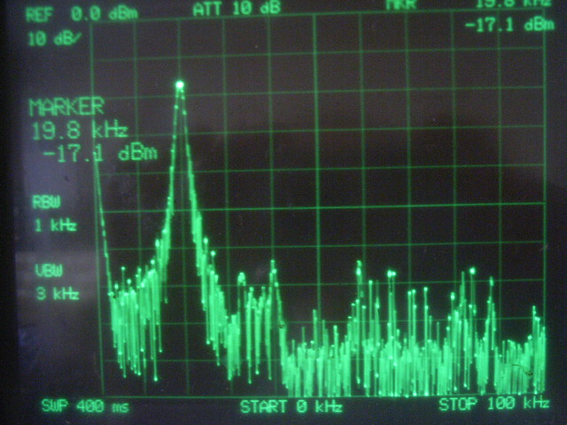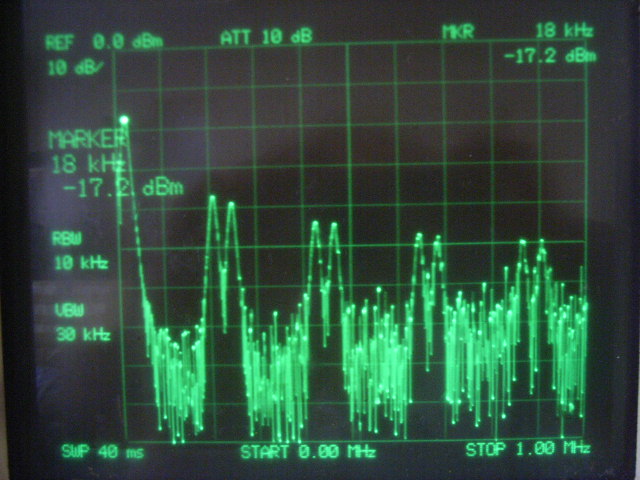
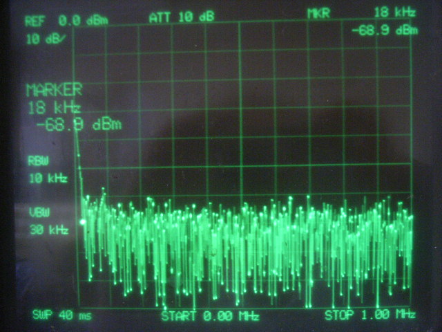
20KHz input (出力あり) 40KHz input(出力無し)
|
1.なんとか、できました Memory Usage
INFO: Design contains EBR with ASYNC Reset Mode that has a limitation:
The use of the EBR block asynchronous reset requires that certain timing
be met between the clock and the reset within the memory block.
See the device specific data sheet for additional details.
/fir_rom:
EBRs: 1
RAM SLICEs: 0
Logic SLICEs: 0
PFU Registers: 0
-Contains EBR fir_rom_0_0_0: TYPE= DP16KB, Width_A= 18, Width_B= 2,
Depth_A= 256, Depth_B= 256, REGMODE_A= OUTREG, REGMODE_B= OUTREG,
RESETMODE= SYNC, WRITEMODE_A= NORMAL, WRITEMODE_B= NORMAL, GSR=
DISABLED, MEM_INIT_FILE= fir_256_2.mem, MEM_LPC_FILE= fir_rom.lpc
/sin:
EBRs: 1
RAM SLICEs: 0
Logic SLICEs: 30
PFU Registers: 30
-Contains EBR triglut_1_0_0_0: TYPE= DP16KB, Width_A= 18, Depth_A= 256,
REGMODE_A= NOREG, REGMODE_B= NOREG, RESETMODE= ASYNC, WRITEMODE_A=
NORMAL, WRITEMODE_B= NORMAL, GSR= DISABLED, MEM_LPC_FILE= sin.lpc
/singleRAM:
EBRs: 1
RAM SLICEs: 0
Logic SLICEs: 0
PFU Registers: 0
-Contains EBR singleRAM_0_0_0: TYPE= DP16KB, Width_A= 18, Width_B= 9,
Depth_A= 256, Depth_B= 256, REGMODE_A= OUTREG, REGMODE_B= OUTREG,
RESETMODE= SYNC, WRITEMODE_A= NORMAL, WRITEMODE_B= NORMAL, GSR=
DISABLED, MEM_LPC_FILE= singleRAM.lpc
DSP Component Details
. MULT36X36B mac/dsp_0:
Multiplier
Operation Signed
Operation Registers CLK CE RST
--------------------------------------------
Input
Pipeline
Operation Registers CLK CE RST
--------------------------------------------
Input
Pipeline
Data
Input Registers CLK CE RST
--------------------------------------------
A CLK0 CE0 RST0
B CLK0 CE0 RST0
Pipeline Registers CLK CE RST
--------------------------------------------
Pipe CLK0 CE0 RST0
Output Register CLK CE RST
--------------------------------------------
Output
Other
GSR DISABLED
PLL/DLL Summary
---------------
PLL 1: Pin/Node Value
PLL Instance Name: myPLL/PLLInst_0
PLL Type: EPLLD
Input Clock: PIN clk_c
Output Clock(P): NODE clkop_c
Output Clock(S): NONE
Output Clock(K): NONE
PLL Feedback Signal: NODE clkop_c
PLL Reset Signal: NONE
PLL K Divider Reset Signal: NONE
PLL LOCK Signal: NODE lock
Dynamic Phase Adjust Input 0: NONE
Dynamic Phase Adjust Input 1: NONE
Dynamic Phase Adjust Input 2: NONE
Dynamic Phase Adjust Input 3: NONE
Dynamic Duty Adjust Input 0: NONE
Dynamic Duty Adjust Input 1: NONE
Dynamic Duty Adjust Input 2: NONE
Dynamic Duty Adjust Input 3: NONE
Input Clock Frequency (MHz): 113.6000
Output Clock(P) Frequency (MHz): 56.8000
Output Clock(K) Frequency (MHz): NA
Output Clock(P) Actual Frequency: 57.0000
CLKOP BYPASS: DISABLED
CLKOS BYPASS: DISABLED
CLKOK BYPASS: DISABLED
CLKI Divider: 2
CLKFB Divider: 1
CLKOP Divider: 8
CLKOK Divider: 2
CLKOS Phase Shift (degree): 0.0
CLKOS Duty Cycle (*1/16): 8
Phase_Duty Control: STATIC
FB_MODE: NONE
------------------------------------------------------------------------------- Preference Summary 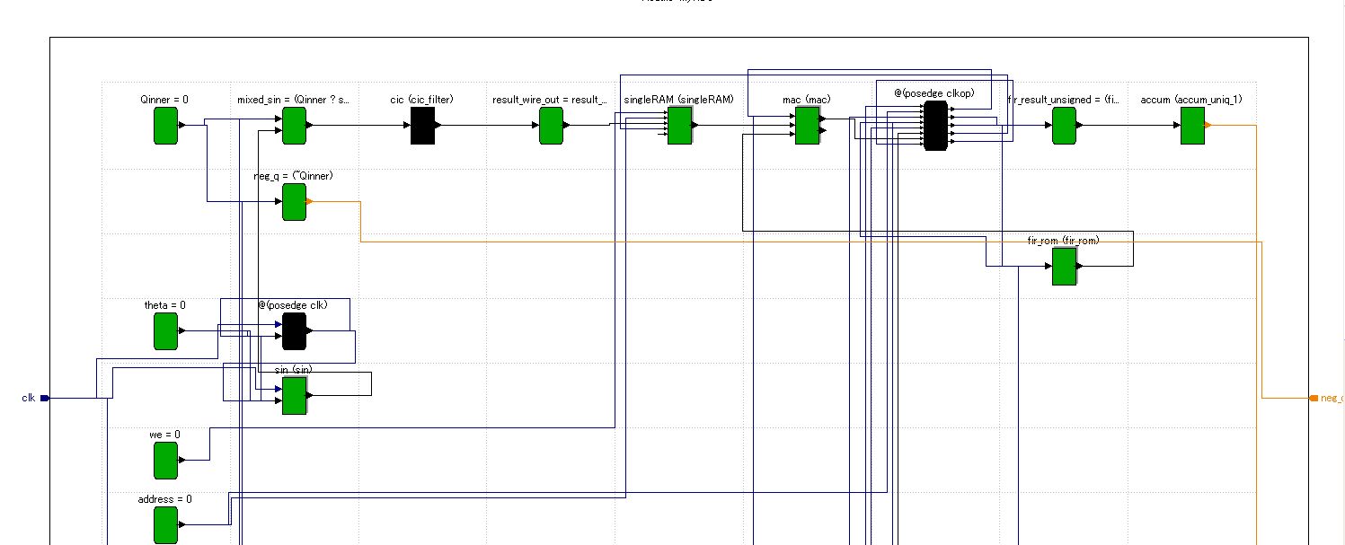 ///////////////////////////////////////////////
verilog HDL 記述 program /////////////////////////////////////////// module myADC( clk,D,neg_q,q ); input
clk; ////////////////////////////////////// reg [19:0]
data=0; singleRAM singleRAM (.Clock(clkop),
.ClockEn(1'b1), .Reset(reset), .WE(we), .Address(address),
.Data(result_wire_out), .Q(q_out)); assign
neg_q=~Qinner; assign fir_result_unsigned=fir_result + 30'h1fff_ffff; accum #( OUTPUT_WIDTH+4) accum(clkop,fir_result_unsigned,q); always @(posedge
clkop) begin end
endmodule
parameter OUTPUT_WIDTH=26; input clk; reg signed[OUTPUT_WIDTH:0]yn=0; always@(posedge
clk) begin end
module accum(clk,VDA,cy_out); parameter
DATA_WIDTH2=18; ///// internal variables
//////// assign cy_out= cy; always @(posedge clk)
begin endmodule
|